Icom IC-7300 Hot-switch Mitigation
The Issue
Unfortunately, there is no similar user adjustable menu setting for controlling the delay time from when the transmitter ceases RF output and the SEND jack commands an external amplifier off. Because the IC-7300 continues to output RF energy while an external amplifier is in the process of switching off, the amplifier's TR/RX relay is subject to hot-switching and the concomitant possibility of arcing at the relay contact points, or worse yet, welding together of those points resulting in the amplifier taken out of service.
This RF-tail issue has been extensively addressed for years by Amateur operators on both the IC-7300 discussion group, and QRZ.COM Forum. Below is finally a possible hardware solution to the hot-switching issue originally suggested by Frank Johnson (G0GSR).
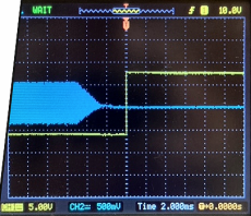
Frank used his oscilloscope to observe the timing of the IC-7300 RF output compared to the SEND relay's opening to switch the external amplifier off. Here's what he found:
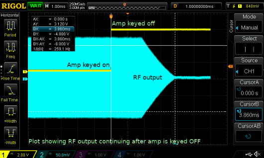
The above o'scope trace shows RF output continuing for ≈3.86 milliseconds after the SEND relay has commanded the amplifier off, thus the amplifier is switching hot RF energy that has the potential to cause arcing of the amplifier's TX/RX relay contacts.
"From the oscilloscope trace, if the antenna relay had been opening early, the output RF would have been abruptly cut-off and it wasn't; it decayed in a controlled manner before the contacts opened."Frank further suggested this possible fix:
"If the logic drive signal for the antenna changeover relay [RL801] driver transistor [Q778] was logic OR'd to that of the SEND relay [RL101] driver [Q101 input] via a diode, the SEND relay would be held energized until the antenna changeover relay was also de-energized. This would not affect the closing of the SEND relay and any TX delay setting, just the [SEND] relay's opening time. The antenna changeover relay's timing is correct; it ceases "With the aid of the IC-7300 schematic circuit diagram provided by Icom, I will attempt to illustrate this possible fix in more detail below.
Proposed Fix
Relay Parameters:
Coil Resistance: 979 Ω
Must Close: 6.75 VDC
Must Open: 0.9 VDC
Driver Parameters:
Maximum Collector Current:100 mAdc
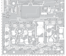

The Send/Receive changeover relay RL801 (Type: FTR-B4CA009Z , depicted on the PA Unit PA2 drawing in the top right area) operates correctly, but the external amplifier SEND relay located on the RF Unit PC board remains on while the IC-7300 continues to output RF energy causing an RF-tail.
It is the output of Q778 that is proposed to be connected to the cathode of the new ORing diode.
It is the input of Q101 (HSENI line ) that is proposed to be connected to the anode of the new ORing diode. The IC-7300 schematic circuit diagrams indicate (on page 8), that the HSENI line that controls the SEND relay originates in IC301, the Main ARM CPU type R7S721000VCFP.
It is the input of Q101 that is proposed to be connected to the anode of the new ORing diode.
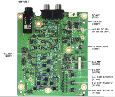
It is the input of Q101 that is proposed to be connected to the anode of the new ORing diode.

This information is provided for a complete understanding of the electrical circuit.

The proposed ORing diode is to be connected between the PA Unit PC board and the RF Unit PC board. To reduce the possibility of unwanted RF coupling through the new diode, it is recommended that the diode be sleeved with copper braid electrically isolated from the diode and connected to chassis ground. If the total length of the diode and its leads are within a piece of heat-shrink tubing, perhaps a piece of RG-174 with its center conductor removed could be slid over the insulated diode to effect the desired shielding. Then the shield braid could be electrically connected to chassis ground while braid ends are free from any electrical contact.
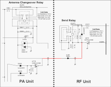

The cathode of the new diode is connected to the output of the IC-7300 Antenna Changeover Relay RL801 driver transistor Q778 located on the PA Unit .
The anode of the new diode is connected to the output of the IC-7300 SEND relay RL101 driver transistor Q101 located on the RF Unit effectively ORing it as described above.
The drawing to the left indicates that the OD of the 1N914 diode is ≈0.06 inches.
The drawing on the right indicates that the ID of the shield braid is ≈0.06 inches.
So, the coax should sleeve over the diode without too much difficulty.

I did the mod and it works perfectly! Thanks so
much for sharing.
73 - Bill
W1BG"
wdgarf@gmail.com
|
|
 |
Frank"
The diode was "just in case". It was easier to include a diode than do proper testing to find out if it was required.
I thought that Icom may be doing something odd with the amp relay closeure timing.
They are driving the two relays separately from two logic signals for some reason known only to themselves?
The same is happening on the IC-9700 and IC-705 which both also have the amp timing fault.
Frank